 | –≠–ª–µ–∫—Ç—Ä–æ–Ω–Ω—ã–π –∫–æ–º–ø–æ–Ω–µ–Ω—Ç: AM50-0003 | –°–∫–∞—á–∞—Ç—å:  PDF PDF  ZIP ZIP |

High Dynamic Range Low Noise Amplifier
800 - 1000 MHz
AM50-0003
M/A-COM Inc. and its affiliates reserve the right to make changes to the
product(s) or information contained herein without notice. M/A-COM makes
no warranty, representation or guarantee regarding the suitability of its
products for any particular purpose, nor does M/A-COM assume any liability
whatsoever arising out of the use or application of any product(s) or
information.
∑ North America Tel: 800.366.2266 / Fax: 978.366.2266
∑ Europe Tel: 44.1908.574.200 / Fax: 44.1908.574.300
∑ Asia/Pacific Tel: 81.44.844.8296 / Fax: 81.44.844.8298
Visit www.macom.com for additional data sheets and product information.
V4
1
Features
∑ Low Noise Figure: 1.2 dB
∑ High Input: +18 dBm at 8 V, 60 mA bias
+6.5 dBm at 3 V, 20 mA bias
∑ High Gain: 15 dB
∑ Single Supply: +3 to +8 VDC
∑ Low Cost SOIC-8 Plastic Package
∑ Adjustable current: 20 to 80 mA with external
resistor
Description
M/A-COM's AM50-0003 is a high dynamic range,
GaAs MMIC, low noise amplifier in a low cost, SOIC
8-Lead, surface mount, plastic package. It employs
e x t e r n a l i n p u t m a t c h i n g t o o b t a i n
optimum noise figure performance and operating
frequency flexibility. The AM50-0003 also
features flexible biasing to control the current
consumption vs. dynamic range trade-off. The
AM50-0003 can operate from any supply voltage in
the 3V to 8V range. Its current can be
controlled over a range of 20 mA to 80 mA with an
external resistor.
The AM50-0003 is ideally suited for use where low
noise figure, high gain, high dynamic range, and low
power consumption are required. Typical
applications include receiver front ends in AMPS,
GSM, and ETACS base stations. It is also useful as
a gain block, buffer, driver, and IF amplifier in both
fixed and portable cellular and 900 MHz ISM
systems.
The AM50-0003 is fabricated using a low-cost 0.5-
micron gate length GaAs process. The process
features full passivation for increased performance
reliability. The AM50-0003 is 100% RF tested to
ensure performance specification compliance.
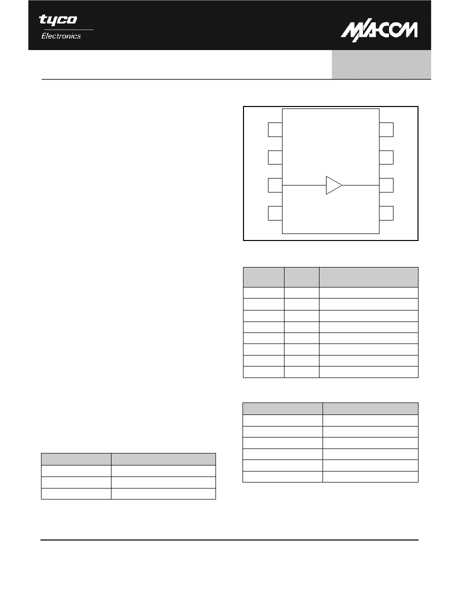
Pin Configuration
Pin No.
Pin
Name
Description
1
GND
RF and DC Ground
2
R
EXT
External Current Control (optional)
3
RF IN
RF Input of the amplifier
4
GND
RF and DC Ground
5
GND
RF and DC Ground
6
RF OUT
RF Output of the amplifier
7
V
DD
Positive supply voltage
8
GND
RF and DC Ground
Ordering Information
Part Number
Package
AM50-0003
Bulk Packaging
AM50-0003TR
1000 piece reel
AM50-0003SMB
Sample Test Board
Note: Reference Application Note M513 for reel size
information.
Absolute Maximum Ratings
1
Parameter
Absolute Maximum
VDD
+10 VDC
Input Power
+17 dBm
Current
2
120 mA
Channel Temperature
3
+150∞C
Operating Temperature
-40∞C to +85∞C
Storage Temperature
-65∞C to +150∞C
1. Exceeding any one or combination of these limits may cause
permanent damage.
2. When pin #2 is used to increase current. (see note 6)
3. Thermal resistance (
jc) = +88∞C/W
Functional Block Diagram
GND
R
EXT
RF IN
GND
GND
RF OUT
V
DD
GND

High Dynamic Range Low Noise Amplifier
800 - 1000 MHz
AM50-0003
M/A-COM Inc. and its affiliates reserve the right to make changes to the
product(s) or information contained herein without notice. M/A-COM makes
no warranty, representation or guarantee regarding the suitability of its
products for any particular purpose, nor does M/A-COM assume any liability
whatsoever arising out of the use or application of any product(s) or
information.
∑ North America Tel: 800.366.2266 / Fax: 978.366.2266
∑ Europe Tel: 44.1908.574.200 / Fax: 44.1908.574.300
∑ Asia/Pacific Tel: 81.44.844.8296 / Fax: 81.44.844.8298
Visit www.macom.com for additional data sheets and product information.
V4
2
Electrical Specifications: T
A
= +25∞C, Z
0
= 50 , F=900 MHz, P
in
= -30 dBm
Parameter
Test Conditions
Units
Min
Typ
Max
Gain
5 V, 60 mA
4
dB
13
15
--
3 V, 20 mA
dB
12
13.5
--
Noise Figure
5 V, 60 mA
4
dB
--
1.20
1.50
3 V, 20 mA
dB
--
1.25
1.50
Input VSWR
--
Ratio
--
2.0:1
--
Output VSWR
--
Ratio
--
1.5:1
--
Output 1 dB Compression
5 V, 60 mA
4
dBm
--
16.5
--
3 V, 20 mA
dBm
--
8.5
--
Input IP3
5 V, 60 mA
4
dBm
12.5
15
--
3 V, 20 mA
dBm
4.0
6.5
--
Reverse Location
--
dB
--
25
--
4. Using external 15 Ohm resistor. See functional bolck diagram herein.
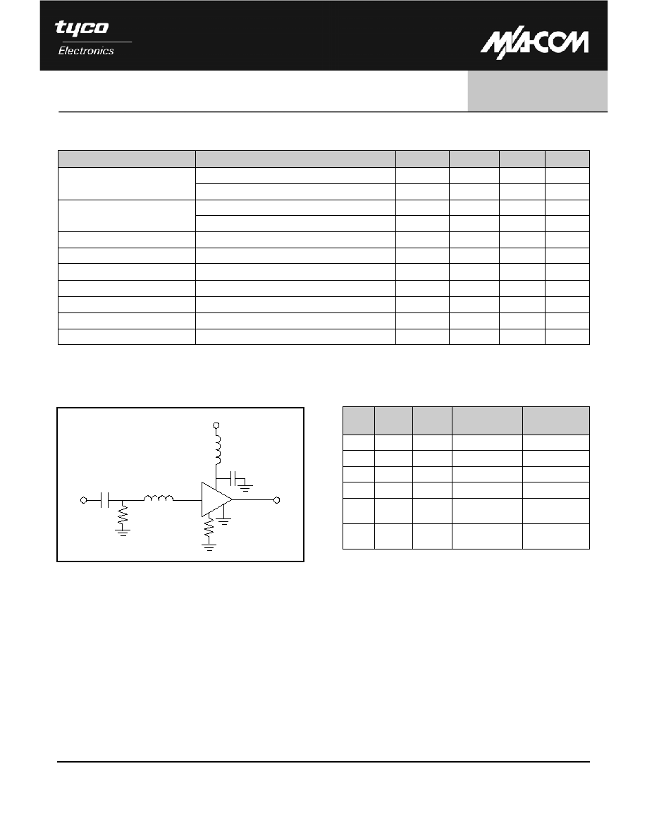
Component List
5
Part Value Case
Size
Manufacturer
Purpose
C1
47 pF
0603
Murata
DC Block
C2
470 pF
0603
Murata
By-Pass
L1
12 nH
0603
Coilcraft
Tuning
L2
12 nH
0603
Coilcraft
RF Choke
R1
5.1K
Ohms
0603
Panasonic
DC Return
R2
See
Note 6
0603
Panasonic
Optional current
control
5. All External circuitry parts are readily available, low cost
surface mount components (.060 in. x .030 in. or .080 in.
x .050 in.)
6. Pin 2 allows use of an external resistor to ground for
optional, higher current. For 20 mA operation, no resistor is
used.
For IDD ~ 40 mA, R2 = 43 ohms;
IDD ~ 60 mA, R2 = 15 ohms;
IDD ~ 80 mA, R2 = 10 ohms.
Handling Procedures
Please observe the following precautions to avoid
damage:
Static Sensitivity
Gallium Arsenide Integrated Circuits are sensitive to
electrostatic discharge (ESD) and can be damaged by
static electricity. Proper ESD control techniques
should be used when handling these devices.
Functional Schematic
IN
OUT
C1
R1
L1
R2
(See Note 6)
L2
V
DD
1,4,5,8
6
3
7
2
C2

High Dynamic Range Low Noise Amplifier
800 - 1000 MHz
AM50-0003
M/A-COM Inc. and its affiliates reserve the right to make changes to the
product(s) or information contained herein without notice. M/A-COM makes
no warranty, representation or guarantee regarding the suitability of its
products for any particular purpose, nor does M/A-COM assume any liability
whatsoever arising out of the use or application of any product(s) or
information.
∑ North America Tel: 800.366.2266 / Fax: 978.366.2266
∑ Europe Tel: 44.1908.574.200 / Fax: 44.1908.574.300
∑ Asia/Pacific Tel: 81.44.844.8296 / Fax: 81.44.844.8298
Visit www.macom.com for additional data sheets and product information.
V4
3
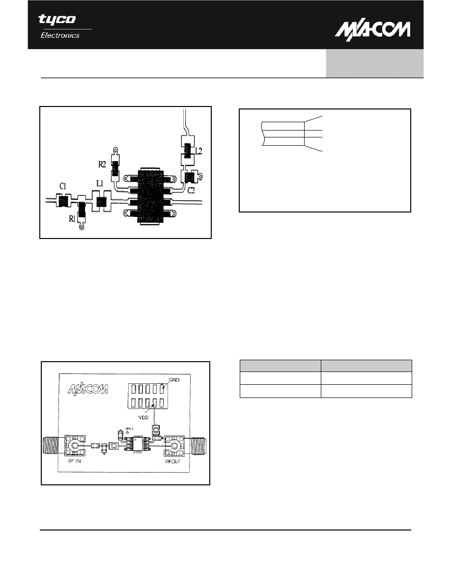
Recommended PCB Configuration
Layout View
The AM50-0003SMB Designer's Kit allows for immediate evaluation of M/A-COM's AM50-0003. The Designer's
Kit includes an evaluation board with mounted AM50-0003 and five loose AM50-0003's. The evaluation board
consists of the recommended external surface mount circuitry, RF connectors, and a DC multi-pin connector, all
mounted to a multi-layer FR-4 PCB. The AM50-0003SMB evaluation PCB is illustrated below with all functional
ports labeled.
Designer's Kit AM50-0003SMB
AM50-0003 Evaluation Board
Evaluation PCB & RF Connector Losses
Port Reference
Approximate RF Loss
LNA Input
0.1 dB @ 900 MHz
LNA Output
0.1 dB @ 900 MHz
The DC connector on the Designer's Kit PCB allows convenient
DC line access. This is accomplished by the one or more of the
following methods.
7.
A mating female multi-pin connector (newark Electronics
Stock # 46F-4658, not included).
8.
Wires soldered to the necessary pins (not included).
9.
Clip leads (not included).
Cross Section View
RF Traces & Components
RF Ground
DC Routing
Customer Defined
The PCB dielectric between RF traces and RF ground layers
should be chosen to reduce RF discontinuities between 50
lines and package pins. M/A-COM recommends an FR-4
dielectric thickness of 0.008" (0.20 mm) yielding a 50 line
width of 0.015" (0.38 mm). The recommended RFmetalization
thickness is 1 ounce copper.

High Dynamic Range Low Noise Amplifier
800 - 1000 MHz
AM50-0003
M/A-COM Inc. and its affiliates reserve the right to make changes to the
product(s) or information contained herein without notice. M/A-COM makes
no warranty, representation or guarantee regarding the suitability of its
products for any particular purpose, nor does M/A-COM assume any liability
whatsoever arising out of the use or application of any product(s) or
information.
∑ North America Tel: 800.366.2266 / Fax: 978.366.2266
∑ Europe Tel: 44.1908.574.200 / Fax: 44.1908.574.300
∑ Asia/Pacific Tel: 81.44.844.8296 / Fax: 81.44.844.8298
Visit www.macom.com for additional data sheets and product information.
V4
4
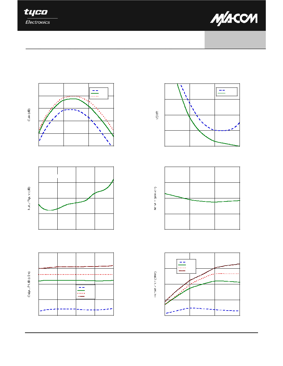
Typical Performance Curves
Test Conditions: T
A
= +25∞C, Z
0
= 50 , V
DD
= 5 V, I
DD
= 60 mA unless otherwise specified
VSWR vs. Frequency
Gain vs. Frequency
Noise Figure vs. Frequency
Noise Figure vs. Current, F = 900 MHz
Output P1 dB vs. Frequency
Output P1 dB vs. Current, F = 900 MHz
12
13
14
15
16
17
0.5
0.7
0.9
1.1
3 Volts
5 Volts
8 Volts
Frequency (GHz)
1
2
3
4
5
0.5
0.7
0.9
1.1
INPUT
OUTPUT
Frequency (GHz)
1
1.1
1.2
1.3
1.4
0.8
0.85
0.9
0.95
1
Frequency (GHz)
Vdd = 3 to 8 Volts
1
1.1
1.2
1.3
1.4
20
40
60
80
IDD (mA)
Vdd = 3 to 8 Volts
8
12
16
20
24
0.8
0.85
0.9
0.95
1
3 VOLT
5 VOLT
6 VOLT
8 VOLT
Frequency (GHz)
8
12
16
20
24
20
40
60
80
3 VOLT
5 VOLT
6 VOLT
8 VOLT
IDD (mA)

High Dynamic Range Low Noise Amplifier
800 - 1000 MHz
AM50-0003
M/A-COM Inc. and its affiliates reserve the right to make changes to the
product(s) or information contained herein without notice. M/A-COM makes
no warranty, representation or guarantee regarding the suitability of its
products for any particular purpose, nor does M/A-COM assume any liability
whatsoever arising out of the use or application of any product(s) or
information.
∑ North America Tel: 800.366.2266 / Fax: 978.366.2266
∑ Europe Tel: 44.1908.574.200 / Fax: 44.1908.574.300
∑ Asia/Pacific Tel: 81.44.844.8296 / Fax: 81.44.844.8298
Visit www.macom.com for additional data sheets and product information.
V4
5
Input IP3 vs. Current, F = 900 MHz
Input IP3 vs. Frequency
5
9
13
17
21
0.8
0.85
0.9
0.95
1
3 VOLTS
5 VOLTS
6 VOLTS
8 VOLTS
Frequency (GHz)
5
9
13
17
21
20
40
60
80
3 VOLT
5 VOLT
6 VOLT
8 VOLT
IDD (mA)
SOIC-8
The AM50-0003 is fabricated using a low-cost 0.5-micron gate length GaAs process. The process features full passivation for increased
performance reliability. The AM50-0003 is 100% RF tested to ensure performance specification compliance.
Typical Performance Curves
Test Conditions: T
A
= +25∞C, Z
0
= 50 , V
DD
= 5 V, I
DD
= 60 mA unless otherwise specified
